page 12 of 33
<< Previous | Next >>
...
Transcript page 12
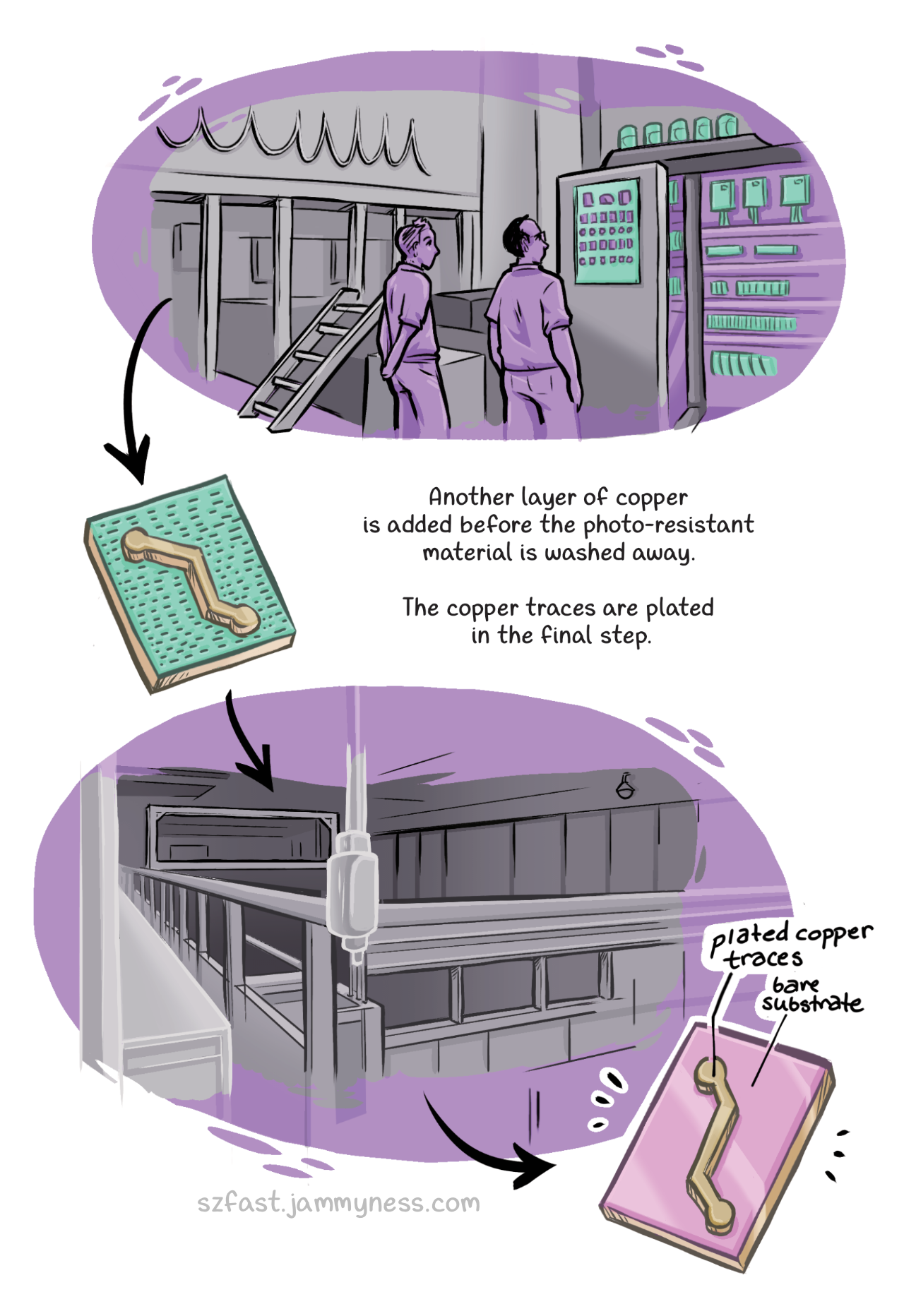
p1: Two workers examine the control panel next to machinery used for copper plating.
Another layer of copper is added before the photo-resistant material is washed away.
p2: A PCB with an extra layer of copper shown on the trace above the photo-resistant material.
p3: A plating bath is shown (t looks like a large pool). The final PCB can be seen with plated copper traces and the bare substrate (PCB material) free of photo-resistant material.
Back to home.