page 11 of 33
<< Previous | Next >>
...
Transcript page 11
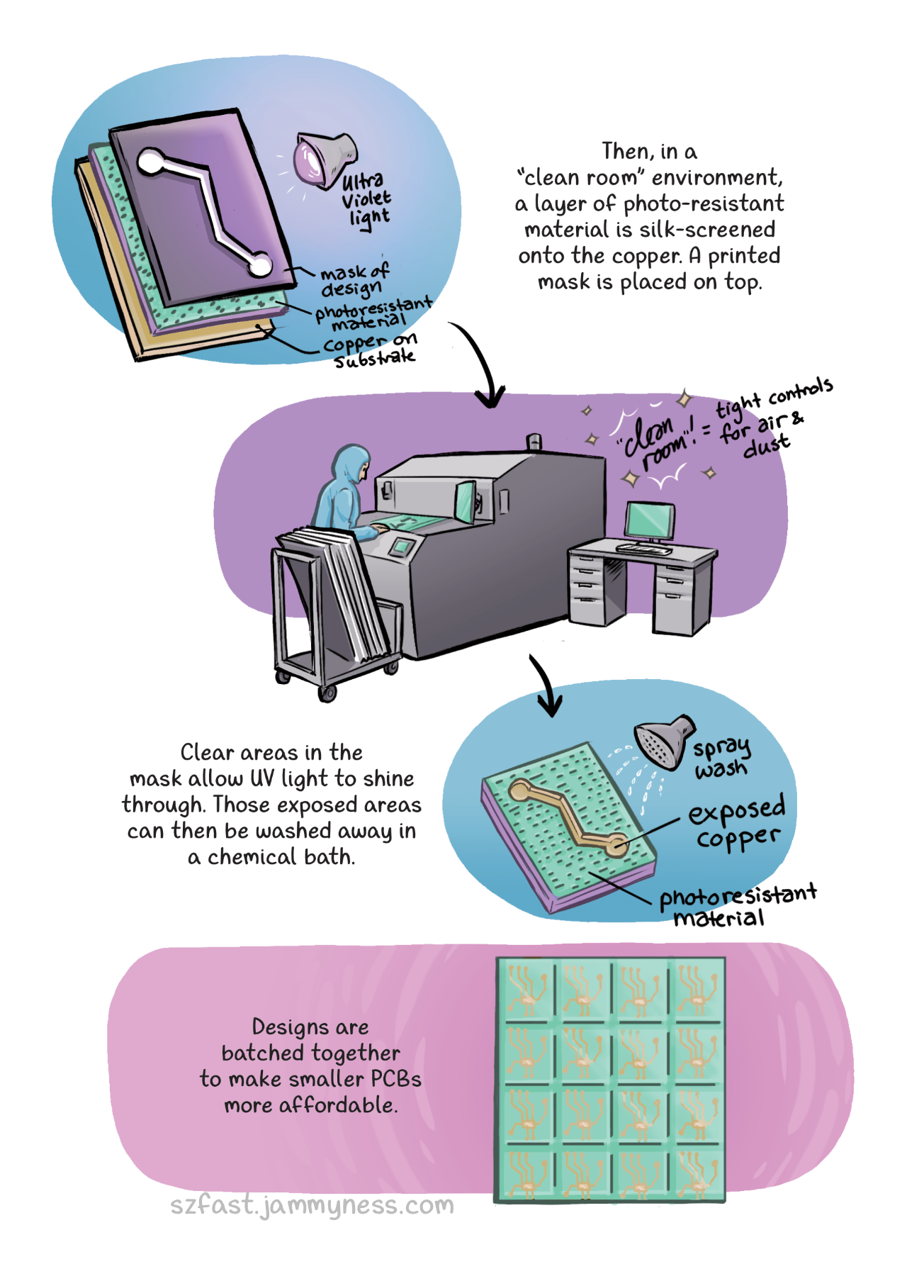
p1: A diagram showing the layers required for the next process: at the bottom is the copper substrate. Above it is a layer of photoresistant material, and on top is a black and clear mask of the intended design. An ultra-violet light is shining on the clear area.
Then, in a "clean room" environment, a layer of photo-resistant material is silk-screened onto the copper. A printed mask is placed on top.
p2: A worker in a "bunny suit" (industrial head-to-toe covering used to ensure the room stays dust-free) stands in front of the photo-resistant printer. They are in a "clean room" which means that it has tight controls for air and dust.
Clear areas in the mask allow UV light to shien through. Those exposed area can be washed away in a chemical bath.
p3: A similar diagram to the layered view in p1, showing how, after UV exposure, a spray wash is used to reveal the exposed copper.
p4: A plate with many small PCB designs copied many times.
Designs are batched together to make smaller PCBs more affordable..
Back to home.